kicad-developers team mailing list archive
-
 kicad-developers team
-
Mailing list archive
-
Message #43153
Re: Back annotate references from PCB
Hi all,
Sorry for big delay in my patch, there's too much ongoing just now and I
had very little time to work on patch ;'-(
Fortunately, I made back annotation patch, witch checks all collisions with
schematic re-usage. Can somebody please have a look on that?
I created the merge request. It passed with warnings, as git checks wants
to mess some old code.
https://gitlab.com/kicad/code/kicad/merge_requests/31
Happy holidays for anybody

On Mon, 2 Dec 2019 at 16:28, Brian Piccioni <brian@xxxxxxxxxxxxxxxxxxxxx>
wrote:

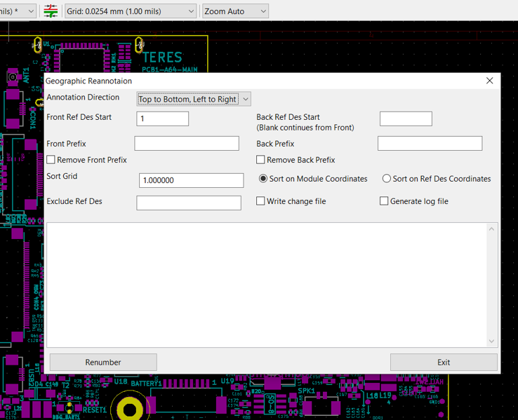
> Thanks to a lot of help from Alexander I have got geographic reannotation
> working. I now have to master git and combine it with his back annotation
> work on eeSchema.
>
>
>
> I have a screen grab attached. My UI design skills are limited by a
> complete lack of artistic skill so comments are welcome.
>
>
>
> I have tested it on all my test boards. It takes less than a second to
> reannotate the TERES laptop (about 500 devices) so I don’t see any point in
> tweaking for performance.
>
> *From: *Alexander Shuklin <jasuramme@xxxxxxxxx>
> *Sent: *December 2, 2019 12:51 AM
> *To: *Vesa Solonen <vesa.solonen@xxxxxxxx>
> *Cc: *kicad-developers <kicad-developers@xxxxxxxxxxxxxxxxxxx>
> *Subject: *Re: [Kicad-developers] Back annotate references from PCB
>
>
>
> Hi all,
>
> I would say, pin swapping is just will be an another tool (you
>
> probably need some specific piece of GUI for that).
>
> The reason I want back-annotation is to have proper geometrical
>
> (geographical) re-annotation. We have contractor who ask if possible
>
> renumber passive components in geometrical order, otherwise assembly
>
> man will get mad when try to solder that by hand.
>
>
>
> On Mon, 2 Dec 2019 at 01:17, Vesa Solonen <vesa.solonen@xxxxxxxx> wrote:
>
> >
>
> > Andy Peters kirjoitti 1.12.2019 klo 21.45:
>
> >
>
> > > Anyway, it’s a lot easier to update the schematic with the new part
> and then forward-annotate, and this keeps both schematic and layout in sync.
>
> >
>
> > Assuming there is the schematic to start with. Sometimes it happens that
>
> > there is just PCB data and one has to go backwards. Commercially that
>
> > rarely makes sense and one may buy pretty extensive reverse engineering
>
> > service form dedicated operators.
>
> >
>
> > > Pin-swapping and gate-swapping are much more important. The pin
> swapping makes for an interesting problem, which is making sure the
> resulting schematic isn’t a mess. Most likely an informal (or required)
> “rule” would be that you draw a net from each pin that can be swapped and
> you give them net labels, but you don’t draw that net to any other pin.
>
> >
>
> > Yes. This is exactly why I see value in a completely bilateral system.
>
> > Drawing a schematic would benefit just as much autorouter as well as
>
> > rubberbanding.
>
> >
>
> > > Thanks to everyone involved in adding the back-annotation feature!
>
> >
>
> > Indeed!
>
> >
>
> > -Vesa
>
> >
>
> > _______________________________________________
>
> > Mailing list: https://launchpad.net/~kicad-developers
>
> > Post to     : kicad-developers@xxxxxxxxxxxxxxxxxxx
>
> > Unsubscribe : https://launchpad.net/~kicad-developers
>
> > More help   : https://help.launchpad.net/ListHelp
>
>
>
> _______________________________________________
>
> Mailing list: https://launchpad.net/~kicad-developers
>
> Post to     : kicad-developers@xxxxxxxxxxxxxxxxxxx
>
> Unsubscribe : https://launchpad.net/~kicad-developers
>
> More help   : https://help.launchpad.net/ListHelp
>
>
>

References