| Thread Previous • Date Previous • Date Next • Thread Next |
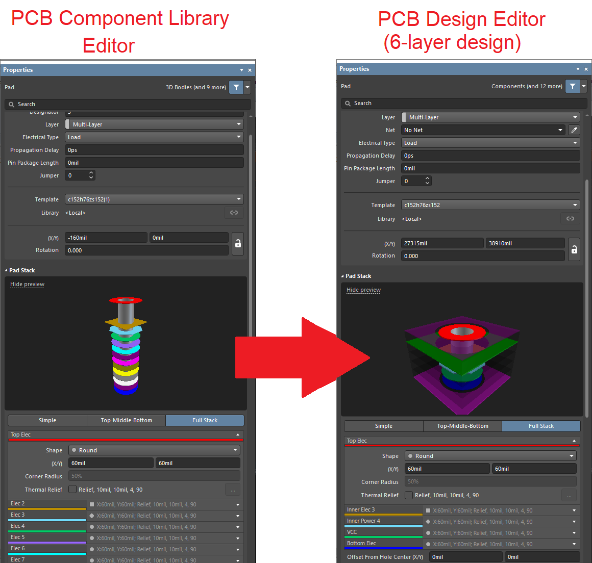
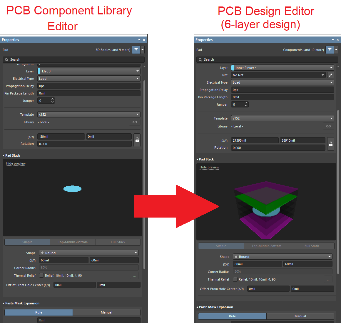
Hi all,

I'm new to the mailing list. I just wanted to make you aware that I'm
starting work on a native Zuken CADSTAR importer for KiCad. I intend to
follow a similar approach to @pointhi in the forums for his Altium importer
- trying to stick to similar class structure where possible. My "short"
term plan is to provide an importer for the CADSTAR PCB archive format
(which is an ASCII file that is based on S-expressions). Since I'm doing
this in my free time, I expect it will take a few months but hopefully the
PCB importer would be ready before KiCad v6 feature freeze. Once I have
something that sort of works, I'll make a merge request and ask for further
feedback on how to improve it.

Now, on a second note, I'd like to provide some input on Pad Stacks. I
joined the mailing list after the last post on the thread "How do we
envision Pad Stacks?" (
https://lists.launchpad.net/kicad-developers/msg44006.html), so I can't
reply to that thread directly, unfortunately. However, the topic discussed
in that thread is very relevant to the work I am trying to do with the
CADSTAR importer (and I bet also important for the Altium importer
@pointhi  made).

I'd like to point out two small inaccuracies in Jon
<https://lists.launchpad.net/kicad-developers/msg44009.html>'s message:


   1. In Altium you *can *define a full pad stack when editing footprints:
   Altium uses a default 14-electrical-layer board stackup which is then
   mapped to whatever layers you actually use in your design when you include
   the footprint.
   2. You *can *define a SMD pad in an inner layer.

Please see attached screenshots from v20.1 showing above two cases, maybe
earlier versions didn't allow this?.  More details can be found here:
https://www.altium.com/documentation/altium-designer/pcb-prop-padpad-properties-ad
.


To keep this email short, I've created a document with other bits of
information that I feel might be useful (such as how CADSTAR handles Pad
Stacks) as well as some suggestions for Pad Stack implementation in KiCad -
maybe this could be the start of a more complex design document?
https://docs.google.com/document/d/1lxBI7_X_I7pO-nuDHPRVlfRBH24XTmwuuN69o_Bqk3s/edit?usp=sharing


Since this mailing list is public, I have made the above link view only
access, but if you'd like to edit, just request it.

Please let me know what you think.

Roberto Fernandez (Qbort)
Attachment:
AltiumDesigner-FullStack.png
Description: PNG image
Attachment:
AltiumDesigner-InnerPad.png
Description: PNG image
| Thread Previous • Date Previous • Date Next • Thread Next |