kicad-lib-committers team mailing list archive
-
 kicad-lib-committers team
-
Mailing list archive
-
Message #00155
Re: Silk screens over pads and naming
On Sat, May 31, 2014 at 12:37:39PM +0100, John Beard wrote:
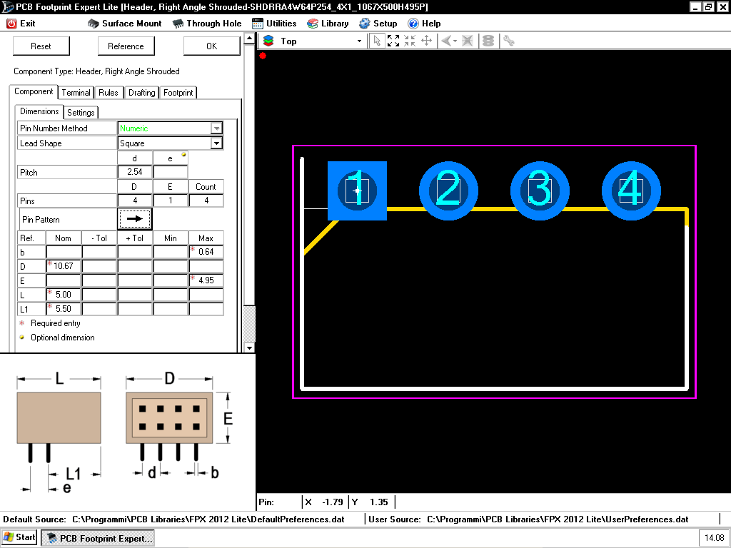
> I'm working on the THT Right-Angle Molex Picoblade headers. I have a
> question about the silk screen.
>
> If you look at the datasheet, the line of the body intersects the pins
> along the back edge. What should I do about the silkscreen in this case?
> Artificially extend it away from the pads (in which case the SS won't
> look like the body), break the line over pads (in which case a SS-only
> view would be full of disjoint lines), or do what I did for now and run
> the line over the pads. The latter has never caused me a problem before:
> most of <well-known proprietary PCB software often used by hobbyists>
> modules do this.
No names made, of course :D
Never used picoblades but know the minispoxs, seems more or less done in
the same way. The issue is that pads are going outside the component
body.
OK, the 7531C rule (the 'modern' one and, in fact, the only standard one
even if it isn't published yet) says that silk should be completely
visible after assembly, and provide a reference mark for pin 1.
So I'd draw an U shape around the outer connector body, with the leg
aside pin 1 longer, to mark the pin. The U horizontal tract would be the
connector 'mouth', and *no* silk on the pin side. I also like to put
a cute arrow on pin 1 on the insertion side, to help connector fitting,
but that's a personal preference.
I'm attaching a quick screenshot of the LP calculator (connector size is
wrong, but the idea is correct): thick white is the silk, thin white is
the body. Pink is courtyard and yellow assembly, but they didn't let me
add them to pcbnew...
Hope it clears the issue.
These slides also explains other 7531C rules (including
thickness): https://communities.mentor.com/mgcx/servlet/JiveServlet/download/28883-8838/PCB%20Design%20Optimization%20Starts%20in%20the%20CAD%20Library.pdf
Of course everything depends on the target technology... if you are
stuck with 5 wires/mm mesh silk screening you can't do 0.15mm silk lines
(for a nominal enviroment). Yes, 7531C is way too modern for some
commonly used processes...
Did we already agree for the 'standard' target process for the default
lib? the baseline commercial cheap process here in Italy is
twoside/0.2: 0.2mm track, 0.2mm clearance, 0.2mm silk screen, 0.2mm
annulus, minimum drill usually 0.4. I think that in the States this
would be known as a 8 mils process. Gives something like 99% yield, so
it's good :D Pads for pitch 0.5 needs to be trimmed but reliability is
good. Also you can rework and patch them by hand easily, without
particular techniques.
For standard work a 0.15 track/clearance no trim for pitch 0.5, and
drill can be usually done to 0.35/0.3 without too much extra cost. Many
rapid proto PCB houses here do this as a standard service at up to
8 layers.
BGA/fine pitch works usually require 0.1 track clearance (and 4 to
...many layers:D). Custom stackups are usually needed or specified
anyway... Microvias are laser drilled at 0.2mm, never seen blind via as
a provided service (YMMV obviously); anyway this kind of board is
definitely *not* a quick turnover product :)
I'd say that targeting for a 0.15mm/6 mil process could be a good
starting point for the 'builtin' libraries.
--
Lorenzo Marcantonio
Logos Srl
Attachment:
connector.png
Description: PNG image
Follow ups
References