kicad-lib-committers team mailing list archive
-
 kicad-lib-committers team
-
Mailing list archive
-
Message #00158
Re: Silk screens over pads and naming
On 31/05/14 13:29, Lorenzo Marcantonio wrote:
Never used picoblades but know the minispoxs, seems more or less done in
the same way. The issue is that pads are going outside the component
body.

OK, the 7531C rule (the 'modern' one and, in fact, the only standard one
even if it isn't published yet) says that silk should be completely
visible after assembly, and provide a reference mark for pin 1.

So I'd draw an U shape around the outer connector body, with the leg
aside pin 1 longer, to mark the pin. The U horizontal tract would be the
connector 'mouth', and *no* silk on the pin side. I also like to put
a cute arrow on pin 1 on the insertion side, to help connector fitting,
but that's a personal preference.
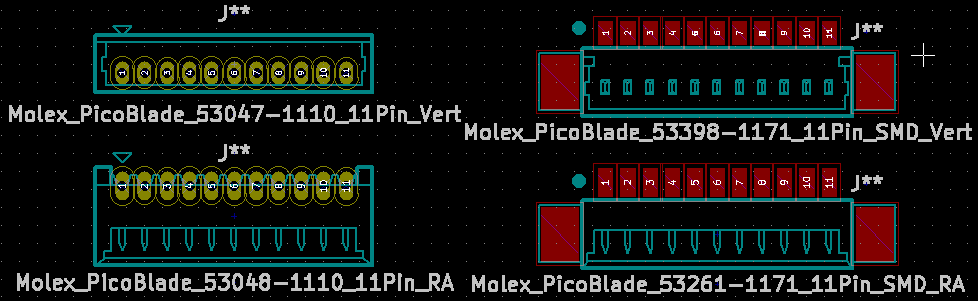
OK, so what I did so far (with a "fancy" silk) is not really what we are
after?

Or, considering that there's no way to add the "body" information except
on the silk, should I keep the fancy silk, which is mostly covered by
the component when assembled, but add the uneven "U shape" as seen in
the Library Expert screenshot? How would that work for the SMD variants,
which have large "wings" for mechanical strength? Would the "U" go
outside these, to the left and right?

I also like the arrow method, or a dot, as you can see.

Cheers,

John
Attachment:
PicoBlade variants.png
Description: PNG image
Follow ups
References