kicad-lib-committers team mailing list archive
-
 kicad-lib-committers team
-
Mailing list archive
-
Message #00173
Re: Silk screens over pads and naming
On 03/06/14 07:42, Lorenzo Marcantonio wrote:
Seems a good starting point to me. Also advanced fabrication requires
often custom-made modules anyway.
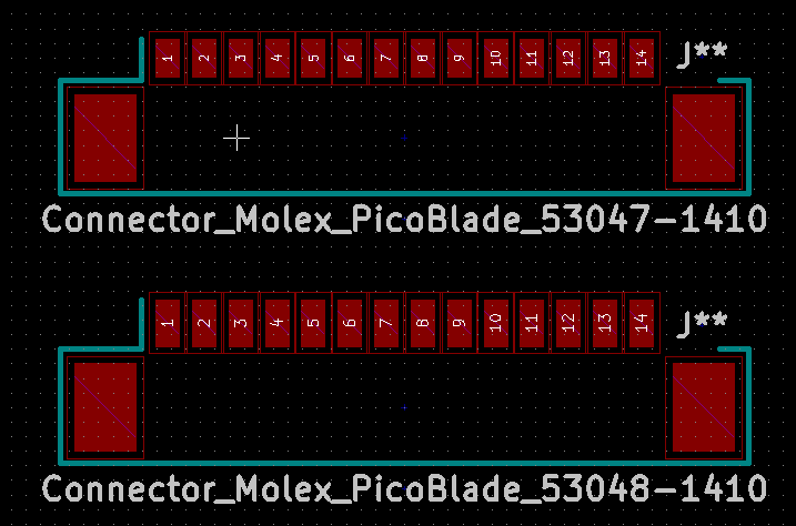
How about this for an example of how the SMD headers would look? I
haven't added the dot/arrow yet, but it basically uses the line
extension at pin 1 idiom from the slides you linked.

If in future we had a way to add assembly data, the graphic of the
connector could be added to that.

This way *does* make it much easier to generate new connectors
programmatically, as there are fewer parameters.

John
Attachment:
Molex simple silk.png
Description: PNG image
Follow ups
References