kicad-lib-committers team mailing list archive
-
 kicad-lib-committers team
-
Mailing list archive
-
Message #00236
Re: Fwd: question about SMD_Packages
On 20/09/14 16:58, Carl Poirier wrote:
Hi folks,

We were unsure how to make the silkscreen for QFN packages. If it's
done the same as TQFP, it yields, for the pin one indication, a bar so
short it's going to be difficult to see. ...... I'm unsure if there
are QFN packages with pins in the reverse order, in which case we
can't tell from the silkscreen.
I've previously been pointed to PCB Libraries' document:
https://communities.mentor.com/mgcx/servlet/JiveServlet/download/28883-8838/PCB%20Design%20Optimization%20Starts%20in%20the%20CAD%20Library.pdf

Their method for QFNs is attached. It's an angle over the corners as
here, but the pin one edge has only one of the lines. The pin without a
line pointing to it is then pin 1.

The same author also previously used a convention of a chamfered corner
(i.e. under the component and symmetrical), with a pin-1 dot, outside
the IPC courtyard in case the pins are numbered in an anti-clockwise
fashion.

http://blogs.mentor.com/tom-hausherr/blog/2011/04/06/pcb-design-perfection-starts-in-the-cad-library-part-15-qfn/

I think the dot is useful, even if the silk outline unambiguously
identified pin 1.
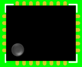
Attachment:
QFN_Silk.png
Description: PNG image
Follow ups
References