kicad-lib-committers team mailing list archive
-
 kicad-lib-committers team
-
Mailing list archive
-
Message #00178
Re: Silk screens over pads and naming
On 03/06/14 09:59, Lorenzo Marcantonio wrote:
> On Tue, Jun 03, 2014 at 09:44:53AM +0100, John Beard wrote:
>> How about this for an example of how the SMD headers would look? I
>> haven't added the dot/arrow yet, but it basically uses the line
>> extension at pin 1 idiom from the slides you linked.
>
> Works for me, could be a good compromise.
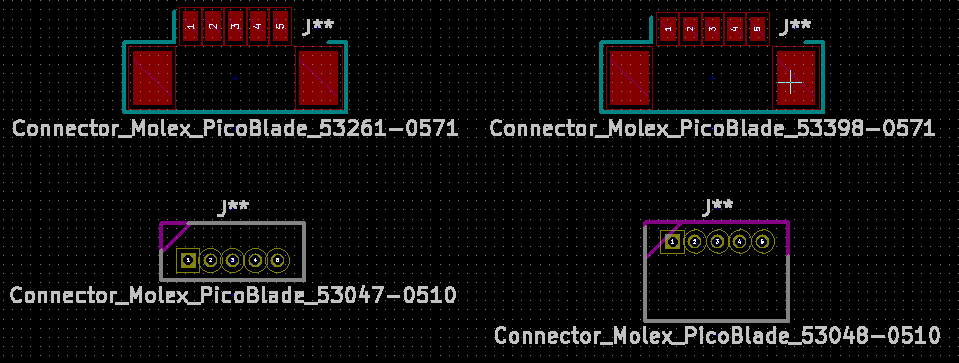
Here is a more up-to-date version of what I have so far. These Molex
PicoBlades are specific instances of more general part generators that
I'm working on.
I have added an assembly layer on F.Adhes (easy to swap out later if
needed). I am not sure what the assembly layer for the SMD components
(with the little "wings") should look like.
Do you think a line/dot on the silk screen is a good idea?
Cheers,
John
Attachment:
PicoBlades new style.png
Description: PNG image
Follow ups
References