kicad-lib-committers team mailing list archive
-
 kicad-lib-committers team
-
Mailing list archive
-
Message #00183
Re: Silk screens over pads and naming
On 05/06/14 08:38, John Beard wrote:
On Tue, Jun 03, 2014 at 09:44:53AM +0100, John Beard wrote:
>
> Here is a more up-to-date version of what I have so far. These Molex
> PicoBlades are specific instances of more general part generators that
> I'm working on.
New version at:
https://github.com/johnbeard/Connectors_Molex.pretty/tree/picoblades
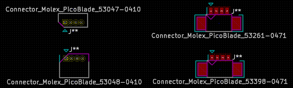
Attached is an image of the 4 styles.
> I have added an assembly layer on F.Adhes (easy to swap out later if
> needed). I am not sure what the assembly layer for the SMD components
> (with the little "wings") should look like.
The wings now look like this:
----------------
----| \ / |----
| v |
----| |----
----------------
I have not marked the protruding legs on the RA assembly: would this be
helpful, as the assembly drawing is not obviously handed? Something
like:
|| || ||
----------------
----| \ / |----
| v |
----| |----
----------------
> Do you think a line/dot on the silk screen is a good idea?
I have added a little triangle arrow at pin 1 for all types, as I think
this is a helpful thing for hand-assembly. I always appreciate it,
anyway!
If people think these are OK, I will go ahead and make the same for
other ranges (e.g. Harwin M40) which have the same general form. I much
rather get this one range nailed down so that all the others can follow
trivially and without too much in the way of changes, which would get
tedious if there are many modules to change in the same way. For example
making the pin 1 marking 50% bigger in each file!
John
Attachment:
PicoBlades new style2.png
Description: PNG image
Follow ups
References